This internship provides a comprehensive introduction to FPGA based digital system design using Verilog. Participants will gain hands-on experience in design, simulation and hardware implementation of digital systems. This program also covers verification techniques and real-time FPGA prototyping, aligned with industry practices.
Key Topics Covered
- Verilog based Digital System Design
- Functional Simulation using QuestaSim
- Testbench Development and Verification Techniques
- Finite State Machine (FSM) Design
- FPGA design & implementation using Vivado
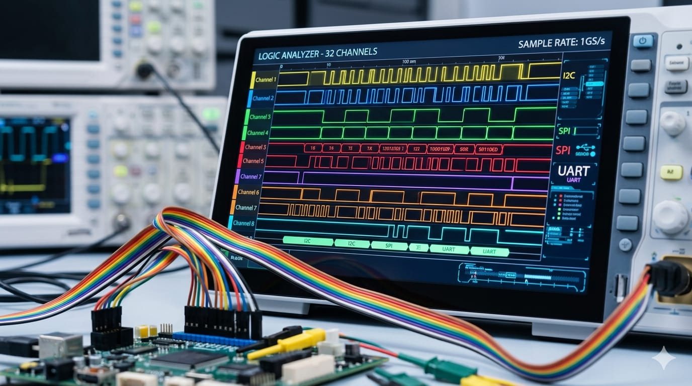
- Hardware Debugging using Logic Analyzer

Program Highlights
- Practical, lab-oriented training
- End-to-end design flow:
Design -> Simulation -> Implementation
- Exposure to industry standard tools
- Certificate on successful completion
Eligibility
Students currently pursuing B.Tech in any semester (Electronics/Electrical) or Engineering Graduates interested in VLSI/FPGA Design
Registration Fee
₹5900 (including GST)
Students can opt for an online two week mini project with an additional fee of Rs. 10,000 if interested.
Venue
C-DAC Technopark Campus
Last Date to Apply
22 April 2026